Bipolar Junction Transistor (BJT) Switch
The Bipolar Junction Transistor can be used as a switch. This is required when the typical digital output (max current output 20ma) does not provide sufficent current drive for high current devices like lamps, solenoids or motors. The transistor current gain provides the order of magnitude increase in collector current.
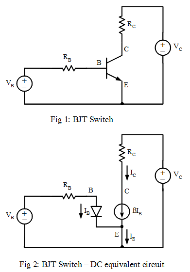
First we redraw the schematic using the BJT DC equivalent circuit
Using KCL (Kirchhoff's current law)
Current through RB
\begin{equation}
I_{RB} = I_B
\end{equation}
Current through RC
\begin{equation}
\label{1}
I_C = \beta I_B
\end{equation}
Current at Node E
\begin{equation}
I_E = I_B + I_C
\end{equation}
Using KVL (Kirchhoff's voltage law) \begin{equation} V_B = I_BR_B + V_{BE} \end{equation} \begin{equation} \label{2} V_C = I_CR_C + V_{CE} \end{equation} Substitute equation \ref{1} into equation \ref{2}: \begin{equation} \label{3} V_C = \beta I_BR_C + V_{CE} \end{equation}
If after substituting circuit values into the equations and we obtain VCE <0 in equation \ref{3} , then the transistor behaves like an on-switch. It is no longer a current controlled current source, and equations \ref{4} and \ref{5} apply instead. \begin{equation} \label{4} V_{CE}=0 \end{equation} Equation \ref{2} simplifies to equation \ref{5} and IC is no longer dependent on IB \begin{equation} \label{5} V_C = I_CR_C \end{equation}
Switching an Inductive Load
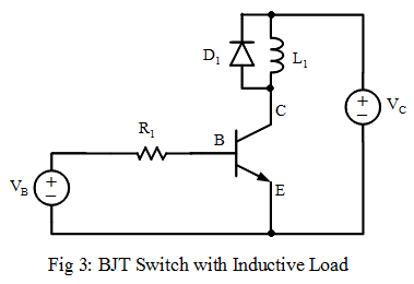
When an inductive load is connected to the collector, a recirculation diode is required across the load to damp the output voltage when the transistor is switched off. When a high current amplification is required, a darlington transistor is used.
Common Emitter Amplifier (BJT)
When a small signal source is connected to the base of the transistor instead of a on/off DC source, the circuit is a common emitter amplifier. To characterise this high gain voltage amplifier involves the AC analysis of the circuit.
Single BJT Circuit Configuration
The Common Emitter BJT Amplifier is one of three single BJT circuit configurations. The other two are the Common Base and Common Collector circuit configurations. Learn the different single BJT configuration and compare their circuit parameters