Digital to Analog Converter
A digital-to-analog converter (DAC, D/A, D2A or D-to-A) is a circuit that converts digital data (usually binary) into an analog signal (current or voltage). One important specification of a DAC is its resolution. It can be defined by the numbers of bits or its step size.
Digital to Analog Converter using the Summing Amplifier
The following diagram shows a 3 bit digital to analog converter implemented using a summing opamp amplifer.
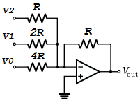
From the summing amplifier circuit (see equation 6), the output voltage is \begin{equation} V_{out} = -R ( {{V_{2}}\over R } + {{V_{1}}\over 2R } + {{V_{0}}\over 4R } ) \end{equation} Simplifying, we obtain \begin{equation} V_{out} = - {1 \over 4} ( 4V_{2} + 2V_{1} + V_{0} ) \end{equation}
| Output Table | ||||
|---|---|---|---|---|
| V2 | V1 | V0 | Digital Value | Vout |
| 0 | 0 | 0 | 0 | 0 |
| 0 | 0 | 1 | 1 | -0.25 |
| 0 | 1 | 0 | 2 | -0.5 |
| 0 | 1 | 1 | 3 | -0.75 |
| 1 | 0 | 0 | 4 | -1.0 |
| 1 | 0 | 1 | 5 | -1.25 |
| 1 | 1 | 0 | 6 | -1.5 |
| 1 | 1 | 1 | 7 | -1.75 |
From the table, we can conclude the following
- The inputs can be thought of as a binary number, one that can run from 0 to 7.
- V2 is the MSB (most significant bit) and V0 is the LSB (least signifcant bit).
- The output is a voltage that is proportional to the binary number input.
- The resolution of this DAC is 3 (the number of bits) or -0.25V (the step size).
- To have more bits, add an additional resistor for each additional bit. Note the relationship between adjacent resistor values.
R-2R Binary Ladder Digital to Analog Converter
The R-2R Digital to Analog Converter uses only two resistance values R and 2R regardless of the number of bits of the converter compared to the summing amplifier implementation where each bit resistor has a different value. The circuit shown is a 3 bit DAC.
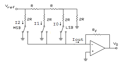
Depending on the state of bit B2, B1 or B0, the respective current I2, I1 or I0 is switched either to ground or to V- of the op amp. Thus \begin{equation} I_{out} = B_2I_2 + B_1I_1 + B_0I_0 \end{equation}
To analyse this circuit, first we observe that since the output is connected to V- through Rf, the opamp is in a negative feedback configuration. Thus \begin{equation} V_- = V_+ = 0 \end{equation}
Therefore the individual current values I2, I1, I0 are unaffected by the switch setting and the resistor network circuit can be redrawn to the following
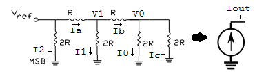
Due to the nature of the resistance network and values, we can obtain the current values by inspection.
From ohms law, \begin{equation} I_0 = I_c \end{equation} From KCL at node V0, \begin{equation} \begin{split} I_b &= I_0 + I_c \\ &= 2I_0 \end{split} \label{5} \end{equation} From KVL, \begin{equation} \label{6} V_1 = I_bR + I_02R \end{equation} Substituting equation \ref{5} into equation \ref{6} \begin{equation} \label{8} V_1 = 4I_0R \end{equation} Again applying ohms law to I1 and using equation \ref{8}, we obtain \begin{equation} V_1 = I_12R = 4I_0R \end{equation} or \begin{equation} \label{10} I_1 = 2I_0 \end{equation} From KCL at node V1, and using equation \ref{5} and \ref{10} \begin{equation} \begin{split} I_a &= I_b + I_1 \\ &= 2I_1 \end{split} \end{equation} From KVL, \begin{equation} V_{ref} = I_aR + I_12R = 4I_1R \end{equation} We leave the reader to figure out how we obtain \begin{equation} I_2 = 2I_1 = 4I_0 = {V_{ref} \over 2R} \end{equation} Thus the R-2R network can be seen to be like a current source whose output depends on switch setting B2, B1, B0 that controls I2, I1, I0 respectively \begin{equation} I_{out} = {V_{ref} \over 8R}(4B_2 + 2B_1 + B_0) \end{equation}
Including the opamp which behaves like I-V converter, we obtain the voltage ouput (note the direction of the current source) \begin{equation} V_{out} = -{{V_{ref}R_f \over 8R}}(4B_2 + 2B_1 + B_0) \end{equation} Letting Vref = 1 and Rf = 2R, we obtain the following output table
| Output Table | ||||
|---|---|---|---|---|
| B2 | B1 | B0 | Digital Value | Vout |
| 0 | 0 | 0 | 0 | 0 |
| 0 | 0 | 1 | 1 | -0.25 |
| 0 | 1 | 0 | 2 | -0.5 |
| 0 | 1 | 1 | 3 | -0.75 |
| 1 | 0 | 0 | 4 | -1.0 |
| 1 | 0 | 1 | 5 | -1.25 |
| 1 | 1 | 0 | 6 | -1.5 |
| 1 | 1 | 1 | 7 | -1.75 |